
ECE 499 Engineering Project
1
2
3
University of Waterloo

Electrical & Computer Engineering
Project Supervisor:
William Wong
ECE 499 Course Coordinator:
Mark Crowley
Abstract
Micro LEDs ($\mu$LEDs) are an exciting, new technology that hold the potential to improve upon the capabilities of the incumbent display technologies of liquid crystal displays (LCDs) and organic light emitting diodes (OLEDs). Researchers and industry leaders deem $\mu$LEDs capable of significant advantages in display technologies particularly with key performance metrics in contrast, colour gamut, pixel response timings, display lifetime, and power consumption. Currently, there are a variety of technical challenges in fabrication to making the dream of $\mu$LED displays a reality. During this research project I aim to assist in developing a process for packaging $\mu$LEDdisplays onto an addressable backplane. To achieve this we use electroplated indium to create a mechanical and electrical connection between the $\mu$LEDs and thin-film-transistor (TFT) backplane.
Acknowledgements
I would like to thank Prof. William Wong for allowing me to participate in his research lab and providing funding for the entire project, Pranav Gavirneni for being a supportive mentor through the entire research project.
Nomeclature
| Symbol | Definition | Unit |
|---|---|---|
| $A$ | Area | $ [\mu m^2] $ |
| $I$ | Current | $ [\mu A] $ |
| $J$ | Current Density | $ [\frac{\mu A^2}{\mu m^2}] $ |
| $V$ | Voltage | $ [V] $ |
| $R$ | Resistance | $ [\Omega] $ |
: Nomenclature Table
Introduction
LEDs are exceptionally efficient when compared to legacy lighting technologies like arc, incandescent, fluorescent lighting, and others. The advantages inherent to the technology have allowed LEDs to enter a variety of light applications like automotive, general lighting, and display backlighting and many other use-cases. [@uLED_review] Conventional inorganic LEDs have MESA dimensions generally greater than $(300\times 300) \mu m ^2$, however $\mu$LEDs target an area below $(100\times 100) \mu m ^2$ to $1 \mu m ^2$ [@parbrook2021micro]
One of the earliest claims to the discoveries of the LED was by Oleg Losev in the 1920s, the work was generally ignored and the conjectured theory for the operation was incorrect, the subsequent research also focused on $\text{SiC}$ and @-@ semiconductors. This era of research was generally impractical and did not produce sufficient light. However, with the arrival of @-@ semiconductors like $\text{GaAs}$, $\text{GaSb}$, $\text{InP}$, and $\text{SiGe}$ there was significant progress in luminosity, although sadly this was all within the infrared spectrum. Visible LEDs would emerge as research in the area quickened, the technology was based on $\text{GaAsP}$ epitaxy over $\text{GaAs}$ substrates. This would bring forth the advent of commercializable LEDs that would now be seen everywhere. Eventually efficiency and luminosity would surpass that of traditional lighting solutions like filament based tungsten and bring us to where we are today with LEDs being used in nearly all lighting and display applications.
Motivation for $\mu$ LEDs as a Technology
LCDs and OLEDs currently dominate the display market, each technology comes with its trade-offs and current innovations with quantum dots and fully addressable back-lit mini-LED panels aim to address some shortcomings concerning contrast, colour accuracy, power consumption, brightness, lifetime, and response times.
$\mu$LEDs aim to address many of these concerns as well, by offering a number of advantages over traditional LCD and OLED displays. The biggest advantage $\mu$LEDs would provide over LCDs is the power efficiency where LCDs suffer from high power loss due to the multiple diffuser and filtering layers required to compose a screen [@LCD_bad]. A commonly cited number is that LCDs loose nearly 70-90% of the flux introduced by the backlight to the various polarizing layers that comprise the display. In contrast, as $\mu$LEDdisplays would be entirely emissive, none of the light would be lost to the conventional filtering layers.
There are a variety of hurdles $\mu$LED technology, many of which arise from the high production cost and the low external quantum efficiency of the technology [@uledhurdles]. As such adoption has been infeasible as yet.
Indium Electroplating
Introduction
As we are attempting to use indium as a diebonding material, there is adequate justification for such use. Indium diebonding comes with a variety of advantages, the first and foremost being that it is a very forgiving material in a wide variety of ways [@indiumCorpBath]. Indium electroplating can be done at room temperature, the material has a useful low melting point of $\approx 150 ^ \circ C$ [@indiumCorpConstants] and is also an incredibly soft and ductile material. Lastly it also is very resistant to forming thick surface oxides and easily wets to surfaces when it reaches its melting temperature [@indium_diebonding].
Due to the many advantages of the material it is an easy choice to begin with to minimize constraints on other portions of the project.
Process
There are a variety of methods for indium electroplating, while I did not select the electroplating process there are a variety of methods available that are commonly used in industry. The largest differences tend to be in what comprises the solution and the operating temperatures.
The indium electroplating process is based on a now industry standard process that is known to yield good results while requiring a minimum of process optimization. Indium easily allows for wafer bumping where the deformability, low melting point, and cold welding properties [@indiumCorpPulsing]. While other alloys consisting of tin and lead or tin, silver, and copper are also used for these processes they come with other disadvantages such as large crystal sizes and high sensitivity to temperature. The plating solution provided by Indium corporation contains
Adapting the indium electroplating process to the E3-3139 and the resources available there, the process is in .
The process used there allows us to electroplate indium onto the substrate that is Chrome-Gold on Sapphire. Gold is an excellent material for indium to easily electroplate onto, and is particularly effective for eutectic bonding for $\text{In}-\text{Au}$ as the alloy that is formed is able to effectively join the wafers [@waferBondingHandbook].
![Eutectic bonding of $\text{In}-\text{Au}$ micro-bumps. Figure from [@waferBondingHandbook]](/assets/img/report_resources/Ch1/indium_bonding.png) {#fig:waferbondingdiagram width=”40%”}
{#fig:waferbondingdiagram width=”40%”}
Existing Setup Description
In summary the process has us prepare the sample with acids before placing into the plating solution. Then the sample holder and sample are submerged in the plating solution and the current source is applied. However, due to cost constraints a voltage source was obtained to perform in place of a current source.
 {width=”45%”}
A current source would have been preferred over a voltage source due to several reasons. Since electroplating is a process where metal ions are deposited on a substrate through the use of an electric current. The amount of metal deposited is directly proportional to the amount of electric charge that flows through the system, which means that controlling the current is crucial for controlling the thickness and quality of the plated layer.
With a current source, the current can be precisely controlled and maintained at a constant level, which results in consistent and uniform plating as a function of time. On the other hand, a voltage source may not provide a consistent current, as the resistance of the plating solution can vary due to factors such as temperature or impurities, leading to poor plating results.
 {width=”30%”}
Another advantage of using a current source is that it allows for better control over the plating process and reduces the risk of over-plating or under-plating. With a voltage source, the voltage applied to the system can cause the plating rate to fluctuate, which can result in uneven thickness or even damage to the substrate. In contrast, a current source ensures a constant and controlled deposition rate, which minimizes the risk of defects or damage to the substrate.
Using a voltage source with an ammeter can be equivalent to a current source in certain situations. This is because the voltage applied to a circuit is directly proportional to the current flowing through it. By measuring the current in the circuit using an ammeter, the current can be controlled by adjusting the voltage. In this way, the voltage source with an ammeter can effectively act as a current source.
 {height=”6cm”}
 {height=”6cm”}
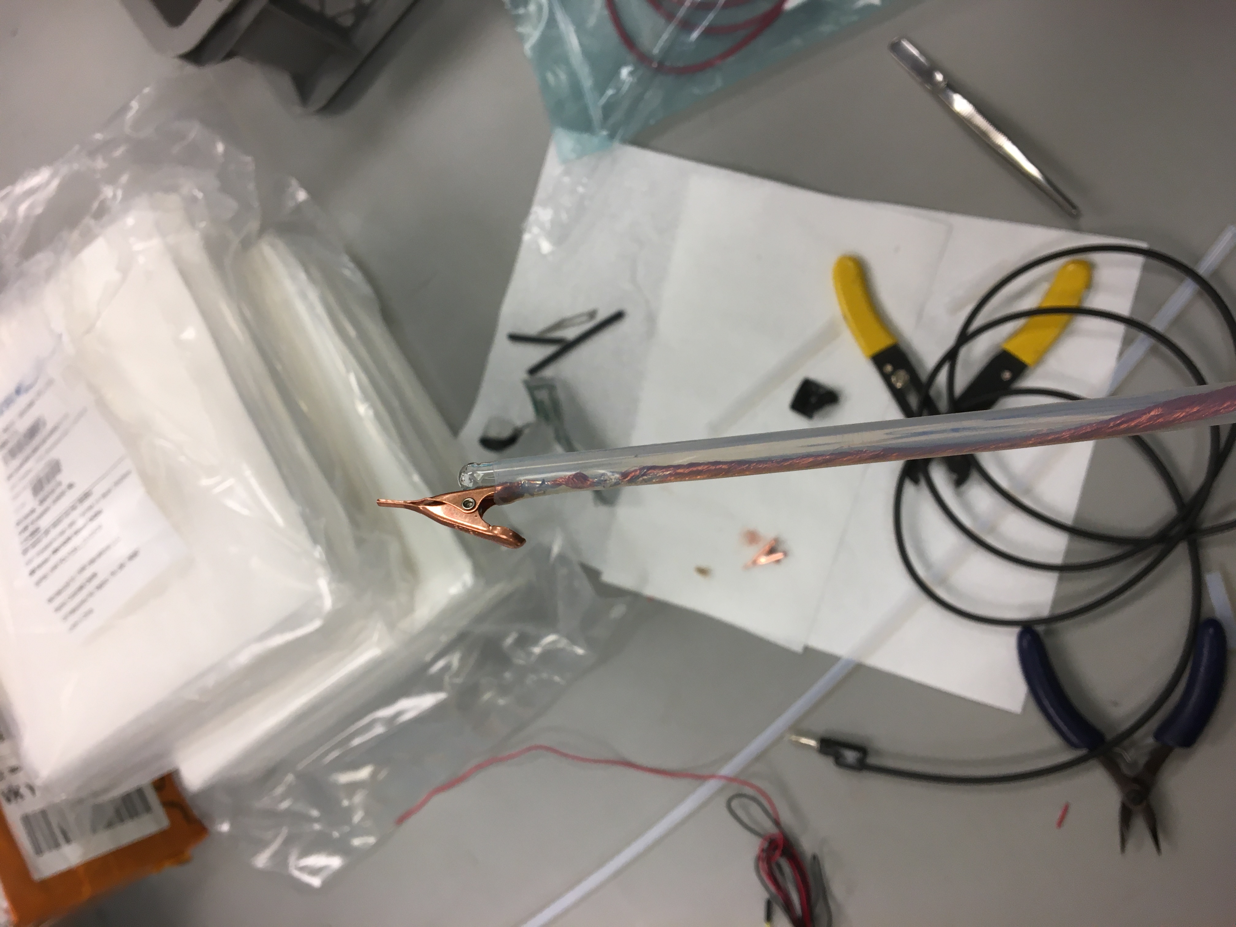
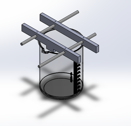
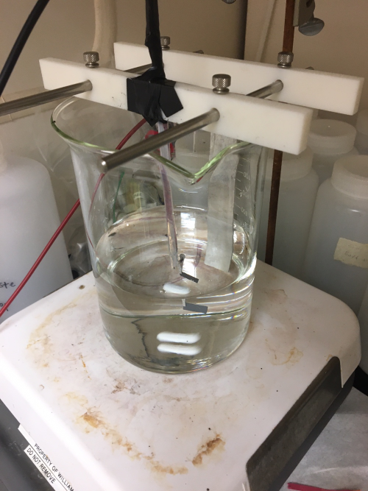
The sample holder consists of two plastic blocks that are held together by two steel bars. Thumbscrews are used to lock the relative position of the plastic pieces in place while the assembly ‘floats’ on the lip of the beaker the sample is submerged into. One of the two plastic pieces has a stopper that helps constrain the position of the assembly on the beaker while the other plastic piece holds the glass rod and alligator clip.
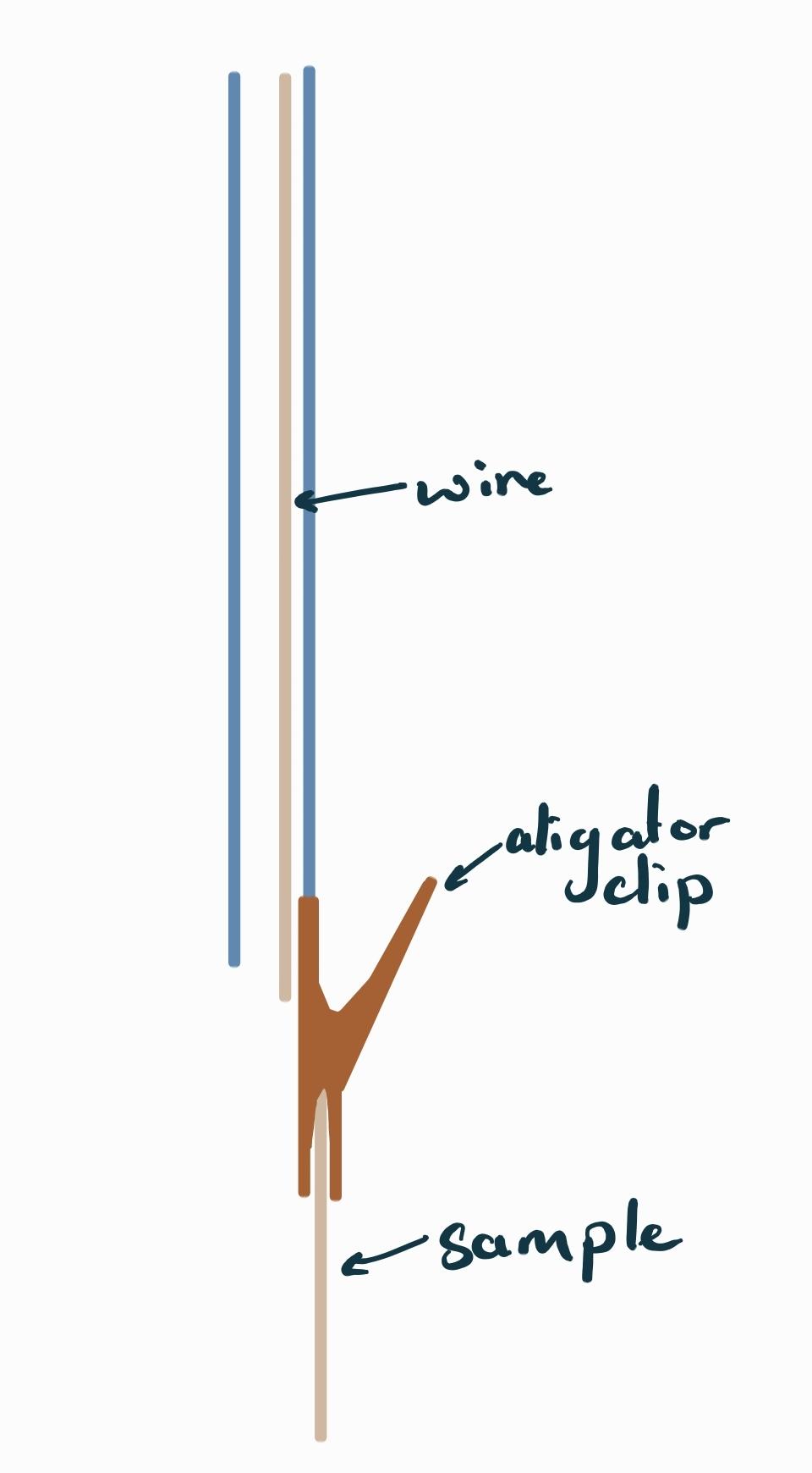
The glass rod is attached to the plastic piece and has the alligator clip on it. The clip and corresponding cathode holder are wrapped in a PTFE sleeve that helps minimize stray electric fields and electroplating onto the cathode wire.
Physical Problems with the setup
The existing setup came with an analog voltage supply that was only able to provide analog control of the voltage based on two knobs (a fine and coarse). This control was only fine enough to $\pm 10 mV$ where the derivative of the current with respect to voltage in the relevant regime was $\frac{d mA}{d mV} = \frac{0.3 mA}{1 mV}$. This meant there was poor resolution on the current control with the previous power-supply with a current resolution of $\pm 3 mA$ which would be an insufficient resolution for the small area that was being plated.
I replaced the existing voltage supply with a Tektronics function generator as it provided an appropriate resolution and dynamic range for such the task. The function generator would allow for pulsed plating as recommended by the indium corporation [@indiumCorpGrainStructure]
Experimental Issues - Deviation from Theory
According to the Indium corporation docs, the recommended electroplating current density for plating is $10-100 \frac{A}{ft^2}$ at $20 \frac{A}{ft^2}$ we should observe plating growth at $1.5 \frac{mm}{hr}$. Converting to SI units from ASME units we see that this yields a plating current of $J_{Plating} \approx 0.11-1.1 \frac{mA}{mm^2}\rightarrow I_{Plating} = 2.907 mA$. However, in this analysis we have only considered the active plating area of the sample, and we have failed to consider the plating area of the exposed alligator clip that holds the sample.
The extra exposed area guarantees an incorrect characterization of the plating growth proportional to the exposed area for the indium bumps. We can show this simply from equation
\[\begin{split} V &\doteq I R \\ I_{Plating} &\doteq J_{Plating} \times A_{Plating} \\ R_{Total} &\doteq R_{Anode} + R_{Plating Solution} + R_{Cathode} + R_{Wires} \\ V_{Plating} &\doteq \text{Variable to satisfy plating current} \end{split} \label{eq:v_eq_ir}\]From the datasheets from Indium Corporation [@indiumCorpPlating] we see that the recommended plating current density.


Or in more elegant units:
\[\notag \begin{split} J_{Plating} &\approx 0.11-1.1 \frac{mA}{mm^2} \end{split}\]We can then solve for the plating current based on the exposed area given by the GDS file of the sample in the gds in chapter 1.
The exposed area is thus:
\[\notag \begin{split} A_{Plating} &= \pi (20 \mu m)^2 + (4.5 mm\times 3 mm) \\ &\approx 13.5 mm^2 \end{split}\]Thus, the plating current for a current density of $20\frac{A}{ft^2}$ or $0.2153 \frac{mA}{mm^2}$ which represents a growth rate of $1.5\frac{mm}{hr}$ or $25 \frac{\mu m }{min}$ is as follows.
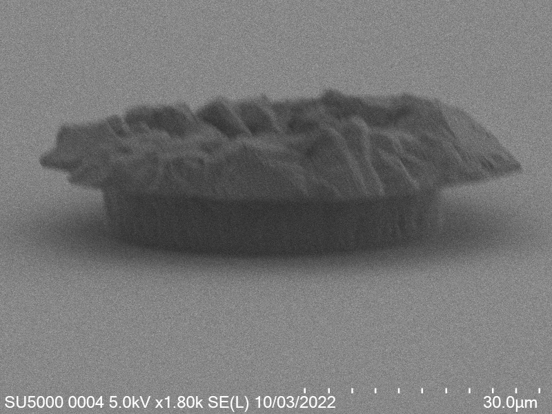
\[\notag \begin{split} I_{Plating} &\doteq J_{Plating} \times A_{Plating} \\ I_{Plating} &= (0.2153 \frac{mA}{mm^2}) \times (13.5 mm^2) \\ I_{Plating} &= 2.907 mA \end{split}\]However, when we apply a voltage of $2.4 mA$ for 5 minutes the growth we see in the $24 mA$ growth figure that the growth is between $0.3-1.2 \mu m$ in thickness.
From those results we can see that the estimate of area that we predicted we got $\frac{0.8}{25} \times 100\% = 3.2\%$ of the expected growth. While that is not explicitly a problem, the indium bumps and growth did not look very uniform or nearly thick enough compared to what would be needed in the proceeding steps.
From here a number of more experiments were conducted and condensed results of the growth were compiled in the plating growths table.
::: {#tab:platingGrowths}
| Sample Name | Electroplating Time ($min$) | Electroplating Current ($mA$) | Indium Thickness ($\mu m$) | Growth rate ($\frac{\mu m}{min} $) |
|---|---|---|---|---|
| 01-Caesar | 5 | 2.4 | 1.1 | 0.22 |
| 02-Augustus | 5 | 2.4 | 0.4 | 0.08 |
| 03-Tiberius | 10 | 2.4 | 1.3 | 0.13 |
| 04-Caligula | 5 | 4.8 | 1 | 0.2 |
| 05-Claudius | 10 | 4.8 | 1.3 | 0.13 |
| 06-Nero | 10 | 9.6 | 1.7 | 0.17 |
| 07-Galba | 5 | 50 | 5 | 1 |
| 08-Otho | 5 | 100 | 14 | 2.8 |
| 09-Vitellius | 5 | 20 | 8.4 | 1.68 |
| 10-Vespasian | 5 | 30 | 8.3 | 1.66 |
| 11-Titus | 5 | 40 | 8.5 | 1.7 |
| 12-Domitian | 5 | 60 | 10 | 2 |
| 13-Nerva | 5 | 20 | 7.6 | 1.52 |
| 14-Trajan | 5 | 20 | 5.6 | 1.12 |
| 15-Hadrian | 5 | 20 | 4 | 0.8 |
| 16-Pius | 5 | 20 | 4 | 0.8 |
: Table of condensed results of Phase 1 plating experiments :::
Development of a Repeatable Process
In summary, the highlighted issues here have to do with the excessive easy by which the sample holder assembly floats on the beaker, this can in instances cause significant change in the plating rate as seen by the large variance in plating rate as seen in the scatter plot figure. I must ensure that the sample is well aligned and distanced appropriately from the indium anode to minimize confounding factors.
Secondly in this section we improved plating current control with the use of a digital function generator and an ammeter in series. With this control of the plating current density was significantly improved by almost 1 order of magnitude.
Phase 1 - Uniform Bonding
Process
The process in this section will aim to first characterize the spread of indium over the surface of the ‘LED’ and ‘backplane’ (‘BP’) substrates 1 and secondly validate uniform bonding over the surface of the sample.
The process that will be used to explore this is the following.
Electroplate indium onto a ‘BP’
Remove photoresist from sample with Acetone then IPA rinse or Remover PG (follow the instructions in [@RemoverPGds])
Do surface activation of LED and BP using the plasma cleaner
Place BP face up and LED face down on diebonder
Using Pick-And-Place (P+P) function on diebonder, pick the LED and place on the BP using the specified bonding pressure and heat recipe
- Bonder Head
Ensure that the bond head being used is a gimbal bond head 2
- P+P
The recipe used on the diebonder for P+P is as following:
Approach and lift the LED using the vacuum function with an application force of $30g$
Complete translational and axial alignment of the LEDs to the BP using the flip-chip camera 3
Ensure the eutectic bonding module is on and set to a place force of $3kg$
Load the correct recipe: $10s \text{@} 60^ \circ C$ followed by $3min \text{@} 250^ \circ C$
After a repeatable electroplating process for indium was developed, the next step was to investigate how the indium would spread once die-bonded. The spreading behaviour of indium is critical because it can impact the performance of the semiconductor device. Specifically, the spreading of indium can affect the heat dissipation and the electrical contact between the die and the substrate. Understanding this behaviour is essential for optimizing the performance of the device. This knowledge can then be used to inform the design and manufacture of semiconductor devices, improving their reliability and performance. Diebonding is the process of placing a semiconductor chip onto a substrate or package, and eutectic bonding is a common diebonding technique. Understanding the behaviour of indium during eutectic bonding is crucial for ensuring the reliability and performance of the final device.
A flipchip diebonder is a machine that is used to bond microelectronic chips directly onto a substrate. It allows for precise alignment and bonding of the chip to the substrate, which is essential for the proper functioning of microelectronic devices. In addition to the standard bonding techniques, a flipchip diebonder with eutectic bonding capabilities enables the bonding of two chips by bonding with precise control of heat and pressure, which can greatly enhance the reliability and performance of the microelectronic device. Eutectic bonding is a specialized technique that involves heating the two materials to their eutectic point, at which they melt and fuse together, creating a bond. 4 This makes the flipchip diebonder with eutectic bonding capability a valuable tool in the field of microelectronics for high-performance and reliable bonding of chips to substrates.
The diebonder being used is the ‘TRESKY-diebond’ tool in the QNC packaging lab it is the Tresky T-3000-FC3 model. The tool is capable of providing a bonding force of up to $490 N$ ($50 kg$ mass) may be applied at temperatures up to $400 ^ \circ C$. The datasheet suggests that it offers placement accuracy of $\pm10\mu m$ [@diebonderDatasheet], While not specified, there are also inherent limitations to the axial accuracy due to the backlash in the gearing of the rotational alignment system.
Characterization of Indium Bonding Spread
In this section, we will explore the characterization of indium spreading during the diebonding process. The primary goal is to gain a deeper understanding of how the indium will melt and spread during the process. We will achieve this by analyzing SEM images of the initial volume and microscope images taken after diebonding. Through this analysis, we aim to identify and quantify the parameters that influence indium spreading and develop an understanding of the fundamental mechanisms involved. The insights gained from this section will help optimize the diebonding process and improve the quality of the final product.
When indium is deposited on a substrate, it forms cylindrical columns that are circular when viewed from the top. During the diebonding process, the indium will melt and spread to form a bond between the substrate and the die. We expect the indium to spread in a circular fashion due to the surface tension of the liquid metal and due to the physical constraints for the material to move when being in essence ‘squeezed’ between two plates. As the indium melts, its surface will try to minimize its surface area and form a shape with the lowest surface area possible, which in this case is a circle. Therefore, understanding the spreading behaviour of the indium is crucial for achieving a successful diebonding process.
Since we want to calculate and understand how the indium will conform when bonding is done, a number of characterization measurements were conducted to understand how the indium will spread and expand over the sample surface. We know the volume of indium will not change when diebonding occurs, we can model the spread of indium as a flattening of a cylinder.
\[\label{eq:radius_indium} \begin{split} V_{Cylinder Initial} &= V_{Cylinder Final} \\ \pi \times r_{Initial}^2 \times h_{Initial} &= \pi \times r_{Final}^2 \times h_{Final} \\ \sqrt{\frac{h_{Initial}}{h_{Final}}} r_{Initial} &= r_{Final} \\ \sqrt{\frac{h_{Initial}}{ 0.65 \mu m}} r_{Initial} &= r_{Final} \end{split}\]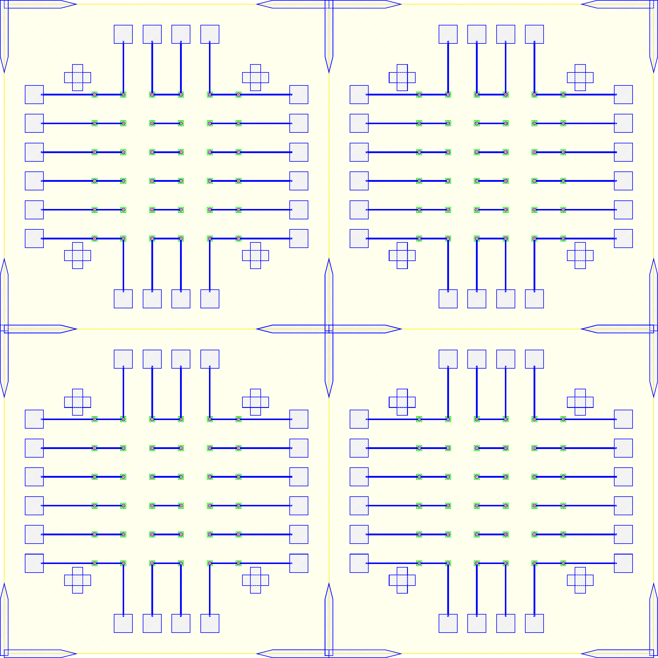 {width=”60%”}
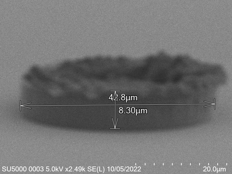
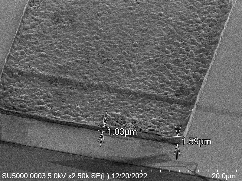
Based on a number of bonding experiments I determined that the average thickness of indium after bonding was around $0.65 \mu m$ a sample of the indium bump can be seen in figure.
The raw data from which the average indium thickness is determined.
::: {#tab:thicknessMap}
| Bond ID | $\text{In}$ Bond Avg. Diameter ($\mu m$) | $\text{In}$ Bump Thickness ($\mu m$) | $\text{In}$ Bump Width ($\mu m$) | $\text{In}$ Bump Volume ($\mu m^3$) |
|---|---|---|---|---|
| BID-005 | 58.6 | 1.3 | 42 | 1801 |
| BID-006 | 84 | 1.7 | 42 | 2355 |
| BID-008 | 200 | 14 | 42 | 19396 |
| BID-009 | 86 | 8.4 | 42 | 11637 |
| BID-010 | 105 | 8.3 | 42 | 11499 |
| BID-011 | 142 | 8.5 | 42 | 11776 |
| BID-012 | 164 | 10 | 42 | 13854 |
: Table of estimated thickness post diebonding :::
From the table after removing outlier values, the median resulting thickness is $~65 \mu m$.
The spread values were identified from images taken from the microscope ‘OLYMPUS-scope3’ in the packaging lab.
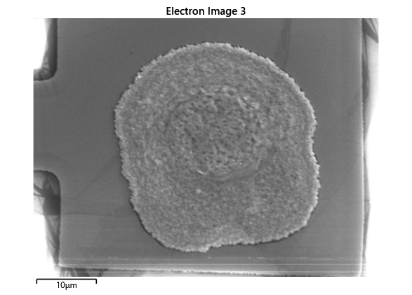
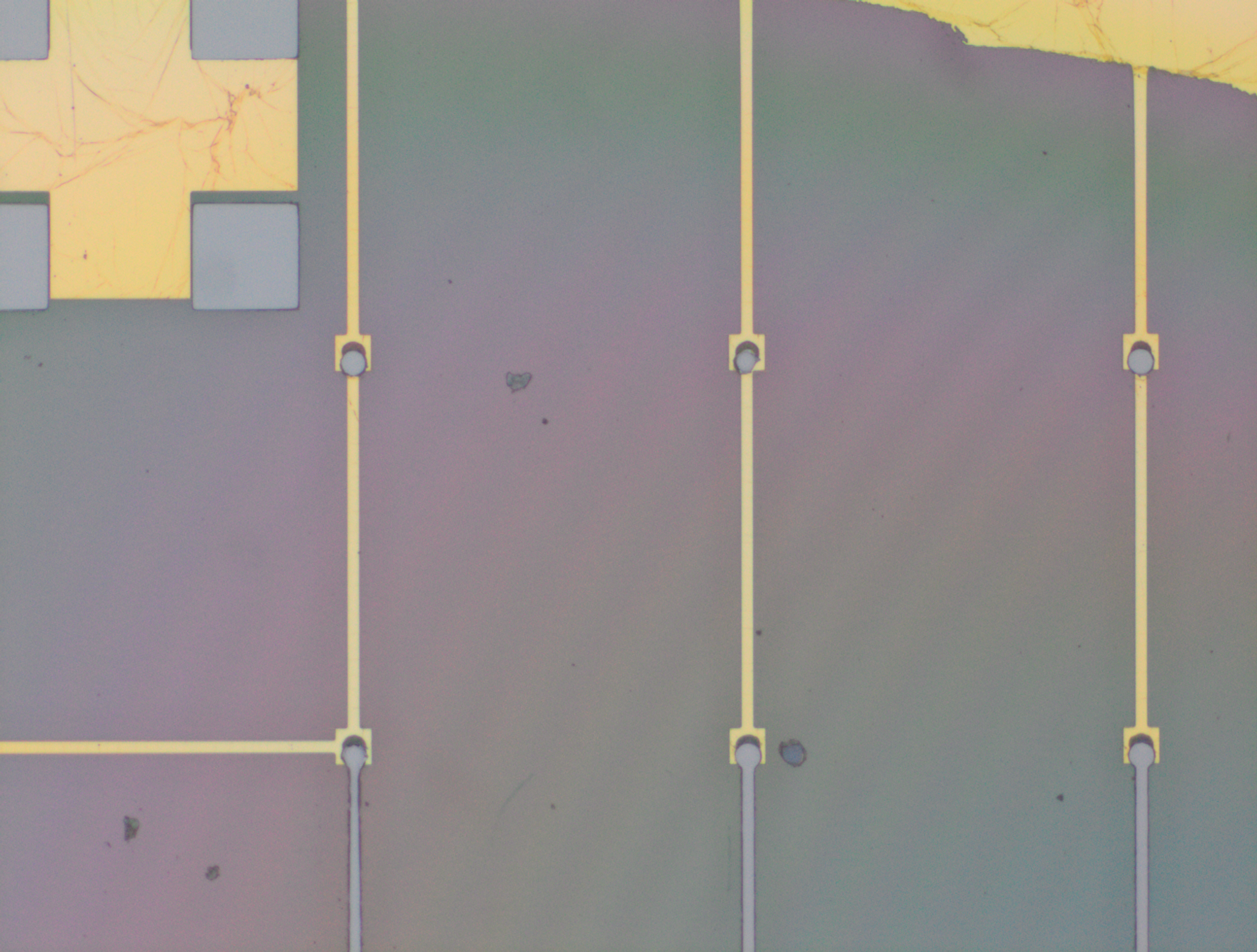
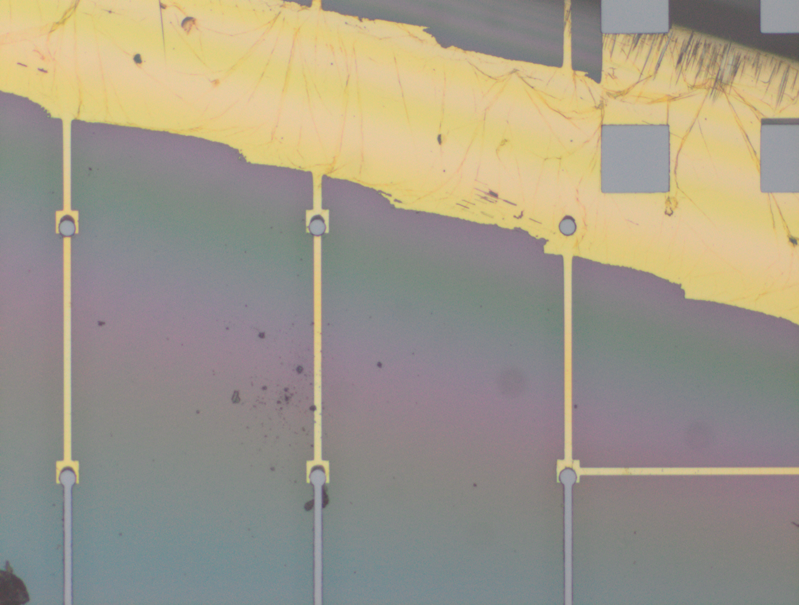
From the images captured by the scope, we can see that the gimbal head in the lab provides sufficiently uniform bonding pressure over the bonding area. The images also show that there is spreading of the indium as the bond is formed directly as a function of the indium volume. This is clear from the fact that the initial electroplated area indicated in a light grey is $42\mu m$ in size and the spread area indicated in dark grey is around $100 \mu m$ in size.
This corresponds to what we see in. Where the initial height of the indium growth from what we expect in where the growth is estimated to be $4-5\mu m$ in thickness.
\[\label{eq:radius_indium2} \begin{split} \sqrt{\frac{h_{Initial}}{ 0.65 \mu m}} 21 \mu m&= r_{Final} \mu m\\ 52.1 &\approx 50 \mu m \end{split}\]Knowing that the bond does spread will constrain the maximum density of $\mu$LEDs for a given bump thickness.


Validation of Uniform Bonding
To validate that the bonding of the LEDs to the BP was uniform microscope images of the bonds were taken from the LED into the bond surface. As the LEDs for this phase of tests are largely transparent and mainly just dots of gold, it is very easy to see the spread of the indium bonds, this can be seen in the images.
The gimbal head that is used has a structure like what is seen in figure allows for ???
Thermal Simulations
Thermal simulations were conducted because there were some bonding failures seen in the samples. As can be seen from SEM images and Energy-dispersive X-ray spectroscopy (EDX or EDS) the indium does not always appropriately wet onto the other substrate being bonded onto this is seen in the SEM images in figure and EDX images in figure. There can be various reasons why indium does not wet onto a surface during diebonding. One reason could be the presence of surface contaminants such as oxides or oils, which can prevent the indium from bonding to the surface. Another reason could be an insufficient amount of heat or pressure during the diebonding process, which can cause the indium to not properly wet onto the surface. Additionally, the surface energy of the substrate can also affect the ability of indium to wet onto the surface during diebonding.
To explore further a lack of heat, thermal simulations were conducted to identify if a process change in the diebonding preprocess was required. Thermal simulations were done in MATLAB with the following code in .
 {#fig:SEM_indium_2 height=”1cm”}
 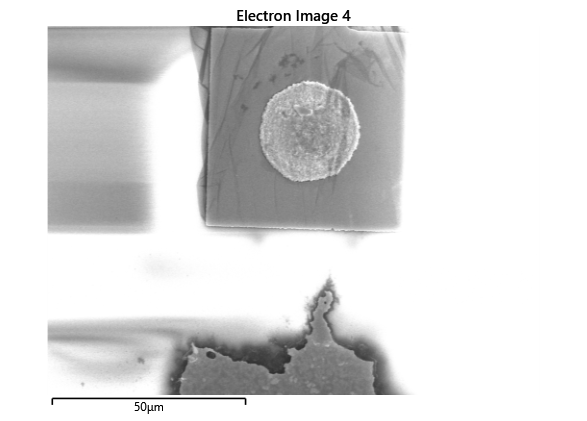 {#fig:SEM_indium_2 height=”1cm”}
 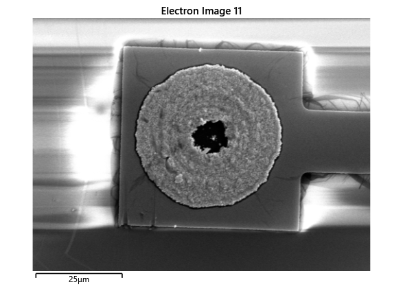 {#fig:SEM_indium_2 height=”1cm”}
 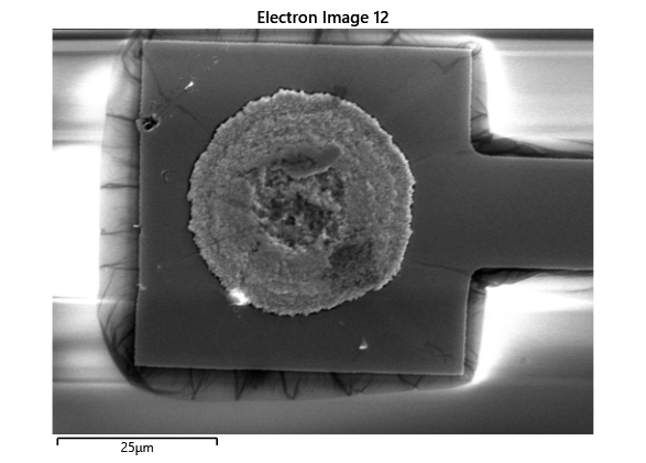 {#fig:SEM_indium_2 height=”1cm”}
 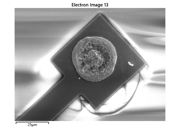 {#fig:SEM_indium_2 height=”1cm”}
 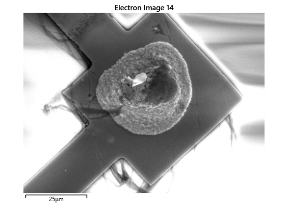 {#fig:SEM_indium_2 height=”1cm”}
 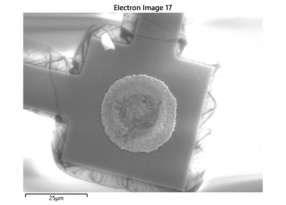 {#fig:SEM_indium_2 height=”1cm”}
 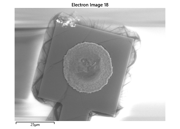 {#fig:SEM_indium_2 height=”1cm”}
 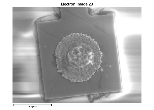 {#fig:SEM_indium_2 height=”1cm”}
  {#fig:SEM_indium_2 height=”1cm”}
  {#fig:SEM_indium_2 height=”1cm”}
  {#fig:SEM_indium_2 height=”1cm”}
  {#fig:SEM_indium_2 height=”1cm”}
 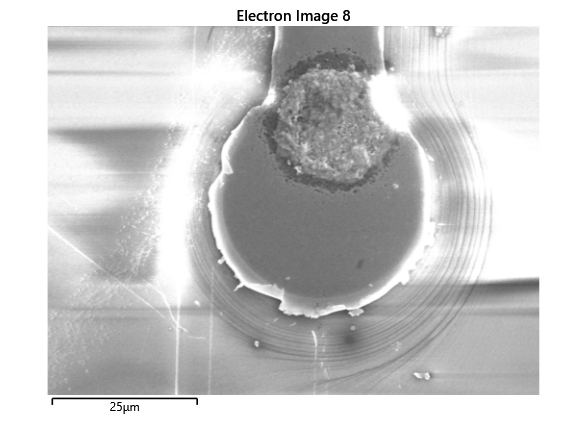 {#fig:SEM_indium_2 height=”1cm”}
 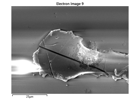 {#fig:SEM_indium_2 height=”1cm”}
 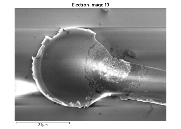 {#fig:SEM_indium_2 height=”1cm”}
 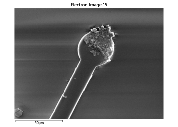 {#fig:SEM_indium_2 height=”1cm”}
  {#fig:SEM_indium_2 height=”1cm”}
  {#fig:SEM_indium_2 height=”1cm”}
  {#fig:SEM_indium_2 height=”1cm”}
  {#fig:SEM_indium_2 height=”1cm”}
 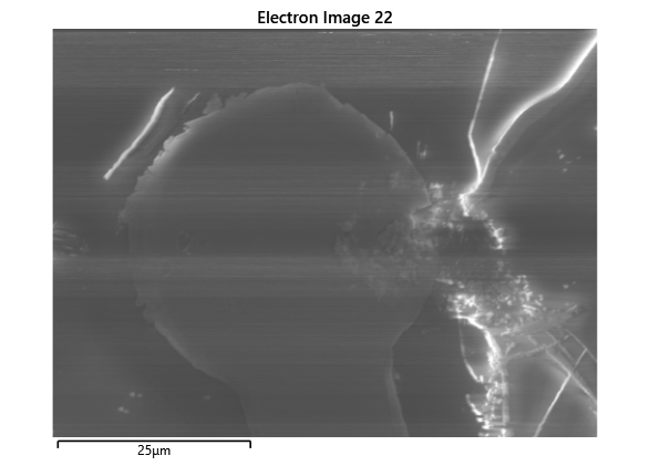 {#fig:SEM_indium_2 height=”1cm”}
 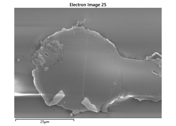 {#fig:SEM_indium_2 height=”1cm”}
 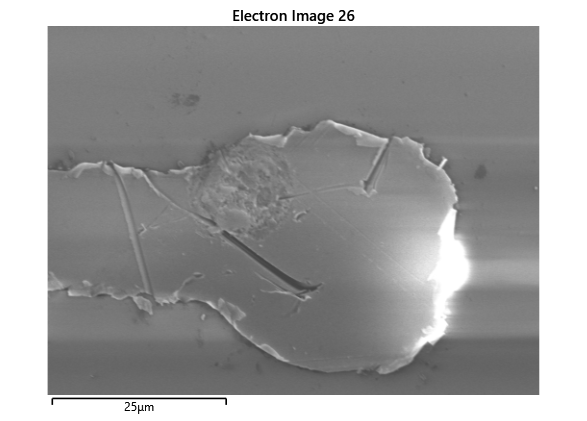 {#fig:SEM_indium_2 height=”1cm”} ———————————————————————————————————————— ———————————————————————————————————————— ———————————————————————————————————————— ————————————————————————————————————————
 {#fig:EDX_indium_2 height=”1cm”}
 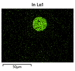 {#fig:EDX_indium_2 height=”1cm”}
 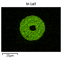 {#fig:EDX_indium_2 height=”1cm”}
 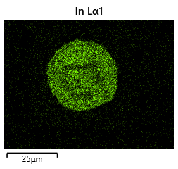 {#fig:EDX_indium_2 height=”1cm”}
 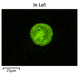 {#fig:EDX_indium_2 height=”1cm”}
 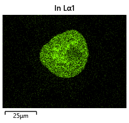 {#fig:EDX_indium_2 height=”1cm”}
 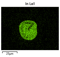 {#fig:EDX_indium_2 height=”1cm”}
 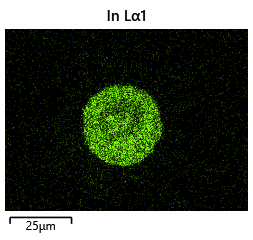 {#fig:EDX_indium_2 height=”1cm”}
 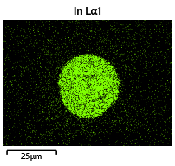 {#fig:EDX_indium_2 height=”1cm”}
 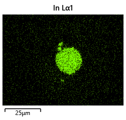 {#fig:EDX_indium_2 height=”1cm”}
 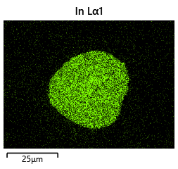 {#fig:EDX_indium_2 height=”1cm”}
 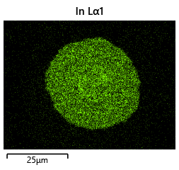 {#fig:EDX_indium_2 height=”1cm”}
 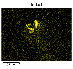 {#fig:EDX_indium_2 height=”1cm”}
 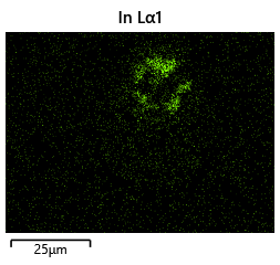 {#fig:EDX_indium_2 height=”1cm”}
 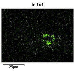 {#fig:EDX_indium_2 height=”1cm”}
 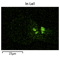 {#fig:EDX_indium_2 height=”1cm”}
 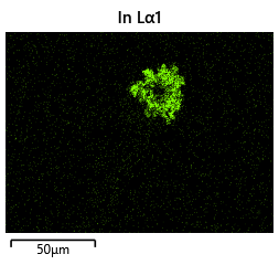 {#fig:EDX_indium_2 height=”1cm”}
  {#fig:EDX_indium_2 height=”1cm”}
  {#fig:EDX_indium_2 height=”1cm”}
  {#fig:EDX_indium_2 height=”1cm”}
  {#fig:EDX_indium_2 height=”1cm”}
  {#fig:EDX_indium_2 height=”1cm”}
 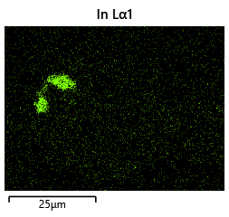 {#fig:EDX_indium_2 height=”1cm”}
 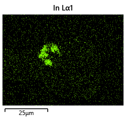 {#fig:EDX_indium_2 height=”1cm”} —————————————————————————————————————————————————————– —————————————————————————————————————————————————————– —————————————————————————————————————————————————————– —————————————————————————————————————————————————————–
The results from the thermal simulations as seen in figure 61{reference-type=”ref” reference=”fig:thermal_simulations”} in MATLAB were that there was more than sufficient time and heat to melt and wet the indium onto the opposing surface. As a result the lack of wetting was likely a result of one of the other issues (contaminants from the flip-chip process or some failure in the surface energies). Both of the other issues are quite possible as during the process the substrate that is bonding onto the substrate with indium on the surface is face down on the ‘diebonder’ which is an unclean surface that also does not have the appropriate surface energies and could dissipate the surface energy generated during the plasma cleaning process.
It can be seen from the thermal simulations that the time taken for the indium to reach temperature is well within $0.3 s$ whereas the bonding recipe calls for the sample to sit at $250 ^ \circ C$ for $5 min$. This is well within 2 orders of magnitude of time for the sample to reach temperature, as such it would be safe to assume that heat/temperature or lack thereof is not the causal source of failure.


Conformation to Theory
In this section we wanted to ensure that there was uniform bonding across the area of the sample, this would arise from the bonding head providing relatively uniform bonding force over the sample area. From the microscope images in the microscope images of the indium we can see that the spread of the indium bumps is uniform over the area of the sample, this would be representative of the gimbal head providing relatively uniform pressure over the face of the sample.
Furthermore, we can also see that the bonding would spread according to the calculated volume. To validate that the indium was spreading as expected, bumps were electroplated to achieve a width of $40 \mu m$. To achieve this we can use equation where we conserve the volume of indium. We can assume that we can consistently generate indium bumps of width $h_{Initial} = 7\mu m$
\[\label{eq:initial_radius} \begin{split} \sqrt{\frac{h_{Initial}}{ 0.65 \mu m}} r_{Initial} &= r_{Final} \\ r_{Initial} &= \sqrt{\frac{h_{Initial}}{ 0.65 \mu m}}^{-1}r_{Final} \\ r_{Initial} &= \sqrt{\frac{7 \mu m}{ 0.65 \mu m}}^{-1} 40 \mu m\\ r_{Initial} &= 12 \mu m \end{split}\]The new GDS files for the altered indium bumps that should achieve a thickness of $40 \mu m$ looks like figure 62{reference-type=”ref” reference=”fig:12um_bumps_gds”}.

After proceeding with the bonding the new images from the microscope look as follows in figure. The images look different as these samples were prepared for the following process in chapter. However, the test for bonding performance is still relevant.
 —————————————————————————————————————————————————- —————————————————————————————————————————————————-
As can be clearly seen in the images that although there is some error in bonding spread, at this scale the placement accuracy limitations play a more significant role and constrain the critical dimension for the bond diameter. Furthermore, the bond size appears to conform to our expectations and reaches a size close to what was predicted.
While the size of the bonds deviate from the preliminary theory this is in part due to the basic modelling of the indium bumps that are assumed to be perfect cylinders. It is clear from the images taken with the SEM that this is not the case and both over plating and under plating cause serious decision from expected results
While results seemed promising with the bonding the bonds from this series of experiments broke very easily. Many of the resulting bonds did not last long enough for the pick and place to remove the head and others failed to last long enough to be transported across the lab to the microscope for imaging of the bonds. In the bond failures section I discuss the method by which the $\text{AuIn2}$ bond forms and why failures occur.
Bond failures
This section will complete a small literature review as to how the bond between the LED and BP forms and why there is failure in the previous experiments.
The Handbook of Wafer Bonding [@waferBondingHandbook] suggests that a typical $\text{In-Au}$ bump consists of a $3\mu m$ thick indium layer and a $0.3\mu m$ thick gold layer. The diagram in part (a) shows what a typical construction of a microbump looks like. While there are differences in the way we construct our bond which looks like. The resulting product should be relatively similar.
As described in the handbook.
In addition, the $\text{Au - In}$ microbump has a relatively low yield strength, and thus undergoes plastic deformation under a mechanical load, which can help relieve mechanical stresses induced in the bonded wafers. The problems of thermal fatigue and creep movement due to the plastic deformation in the $\text{Au - In}$ microbumps can be mitigated by the epoxy adhesive surrounding them.
...
As the temperature increases above $156^ \circ C$, the molten indium dissolves the $\text{AuIn2}$ intermetallic layer to form a mixture of indium - rich liquid with $\text{AuIn2}$ grains. This liquid reacts with the remaining gold layer to form more $\text{AuIn2}$ as shown in Figure 1{reference-type=”ref” reference=”fig:waferbondingdiagram”}(c). Consequently, the composition of $\text{AuIn2}$ in the mixture increases. During cooling to room temperature, the solidification of the mixture starts below $156^ \circ C$ to form indium - rich $\text{Au - In}$ alloys.
Thus, the tensile strength of the alloy is comparable to that of $\text{In}$ which has a tensile strength of $1.6 MPa$ [@indiumCorpConstants] and a shear strength of $6.1 MPa$.
Given that we have a bonded area of:
\[\label{eq:bonded_area} \begin{split} A_{Bonded} &\doteq (6\times 6) \pi r^2 \\ &= (6\times 6) \pi (20 \mu m)^2 \\ &= 45239 \mu m ^2= 0.04524 mm^2 \end{split}\]The tensile strength is given by equation [eq:tensile]{reference-type=”ref” reference=”eq:tensile”}.
\[\label{eq:tensile} \begin{split} \sigma &= \frac{F_{tensile}}{A} \\ 1.6 MPa\times A_{Bonded} &= F_{tensile} \\ 72.4 mN &= F_{tensile} \end{split}\]The calculated tensile strength is extremely low, and the sheer strength is on a similar order of magnitude ($F_{shear} = 276 mN$). This tensile and shear strength is only one order of magnitude greater than the mass of the LED and BP which are $M = \rho_{Sapphire} \times V_{LED + BP} = 0.21 g \rightarrow F_{g} = M g = 2.1 mN$. Due to the inaccuracies of the diebonder we do not observe 100% overlap of the active bonding area which significantly reduces our margins required for maintaining a bond, furthermore the diebonder vacuum system has easily ripped the LED off of a bonded LED and BP pair with sub-nominal vacuum pressure.
Since the current setup fails very easily it requires a solution before we can proceed to the daisy-chain tests in the next chapter. I explain in further detail in the following section how I approached how to resolve this issue.
Development of a Repeatable Process
As previously described a number of bonds did not last long enough for the diebonder to remove the head from on top of the LEDs. While we expected the bonds to be mechanically insecure, we still expected them to handle careful transport for a few days while characterization could be done. Instead, we observed immediate failures. These failures could have been as a result of a variety of reasons, some of these reasons were described in the previous chapter. To avoid tautology the solutions discussed here were to improve the cleanliness of the handling of samples and to increase the bonded area that would bond the LED to the BP.
Adding Anchors
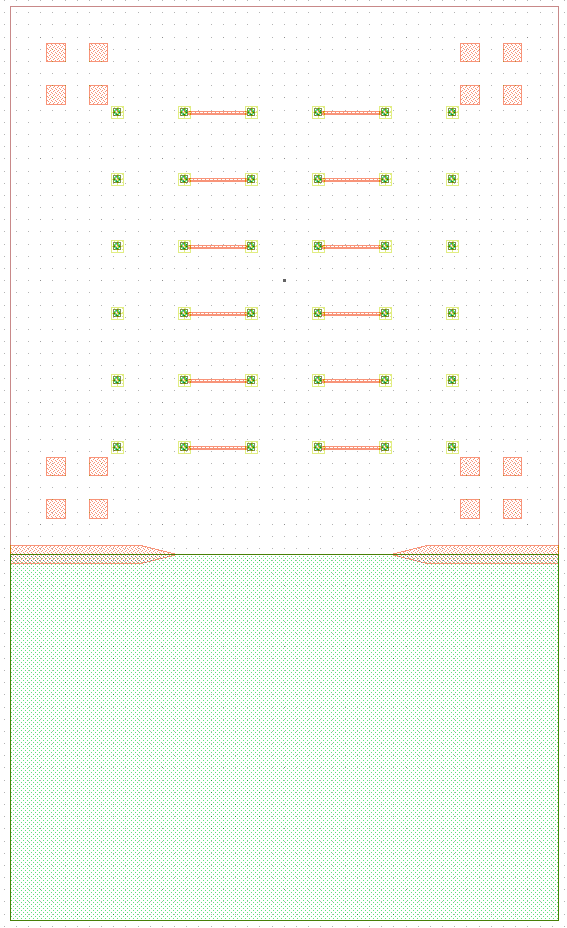
I wanted to add anchors to significantly improve the tensile strength of the bond. To complete this, inactive areas of the LED sample had portions where $\mu$LEDs would not be placed where the $\text{Cr}-\text{Au}$ would not be etched away. Furthermore, on the BP those corresponding areas would have indium electroplated. The corresponding GDS file of the LED and BP look like.
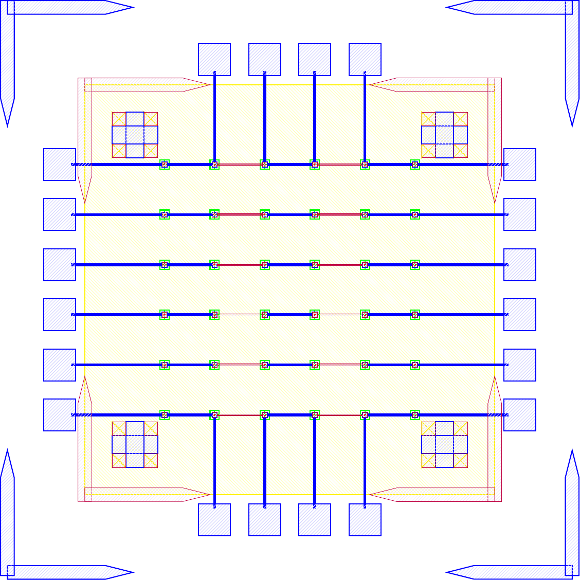
The anchors in figure increase the bonding area by orders of magnitude while maintaining the functionality of the previous design. The new area is given by the folowing.
\[\label{eq:new_area} \begin{split} A_{New} &\doteq \underbrace{(6\times 6) \pi r^2}_{\text{Area of bonds to LEDs}} \underbrace{((5\times 5) 260\mu m\times 40\mu m) + ((2\times 2 \times 4) 150\mu m\times 150 \mu m)}_{\text{Anchors}} \\ &= (6\times 6) \pi (20 \mu m)^2 + 620000 \mu m ^2\\ &= 665239 \mu m ^2= 0.6652 mm^2 \end{split}\]As the new bonded area is well over 14 times greater ($\frac{A_{New}}{A_{Old}} = 14.704$) the corresponding tensile and shear strength should also scale accordingly. As the purpose of this series of experiments is not to develop the strongest possible mechanical bonds between wafers, and the current solution was sufficient for our purposes. No further tests into the strength of bonds were conducted because the bonds held the samples together as seen in figure follwing figures.


Phase 2 - Electrical Connection
Process
In this section we would like to characterize the performance of the electrical connection of the LED to the BP of the process. Since an excellent electrical connection throughout the entire circuit and display is required to power the LEDs and transistors on the backplane it is important to understand the non-idealities that will be encountered in the sample.
To characterize the electrical connection over the sample a daisy-chain test will be conducted [@daisychainTest].
A daisy-chain test for diebonding with indium to bond an LED to a backplane involves bonding a series of LED chips to the backplane sequentially. Each LED chip is bonded using indium diebonding, and the bonding quality and electrical performance of each LED is evaluated before proceeding to bond the next LED in the chain.
The purpose of the daisy-chain test is to ensure that each LED is bonded correctly and functions properly before bonding the next one. This allows for early detection and correction of any bonding issues, and ensures that the final product is of high quality.
We will be using the same GDS file as the one with the added anchors and using a micromanipulator to probe the pads seen on the outside of the GDS file.
Characterization of Electrical Connection
Going through the entire electroplating and diebonding process, I was able to begin the process of characterizing the electrical properties of the diebonds. As I was using the micromanipulator in E3-3177 there were certain limitations and intricacies to using the tool that were not relevant to the characterization, but I felt the need to mention.
The diebonded samples were significantly larger than the field of view of the microscope. This meant I had to translate the sample stage to move the test pads into view.
Some probes suffered from significant static friction and high damping ratio which meant that translation of those probes faced significant lag when being used.
One of the ocular lenses had a focal distance outside the z-axis range of the stage.
The ocular lenses also faced significant vignetting.
Some geared belt drives did not work.
While the previous issues did exist, there were no functional issues with the micromanipulator and the tool was absolutely functional for use in this situation.
Connection Issues
To complete the electrical characterization of the daisy-chain samples, the probes of the micromanipulator were attached to a Kiethley Source Measurement Unit (SMU). The SMU allows us to apply voltages and currents and measure voltages, currents, and resistances. Upon attempting to measure the resistance of the sample, at first an ‘overflow’ or open-circuit was measured.
To overcome this at first a small voltage below $1 V$ and was gradually increased up-to $20 V$ until a current was measured. This procedure of applying a high voltage is likely similar to what is often seen in oxide breakdown of transistors [@oxide_breakdown] where an oxide layer is broken down and promotes the creation of a conductive material from the source to discharge point. However, it is still unclear as to why this surface oxide appears as indium should not have formed a surface oxide layer as according to [@indiumCorpSurfacePrep] an oxide layer of a maximum of $80-100 Å$ would form after $2-4h$ this oxide layer should have been removed by the preceding plasma-cleaning step [@plasma_clean_oxide] and diebonding should have easily melted the indium forming a bond that would work.
Once connection issues were resolved the resistance over the pads were measured. While measuring, however, the resistances over the pads was constantly in flux at a rate of change of $1-4 \frac{\Omega}{min}$.
Conformation to Theory
The results of the measurements were as follows from table
0.3
::: {#tab:daisychain_resistance_table}
| Start | End | Resistance [$\Omega$] |
|---|---|---|
| $v_{i_1}$ | $v_{o_{1,1}}$ | $64$ |
| $v_{i_1}$ | $v_{o_{1,2}}$ | $44$ |
| $v_{i_1}$ | $v_{o_{1,3}}$ | $69$ |
| $v_{i_6}$ | $v_{o_{6,1}}$ | $54$ |
| $v_{i_6}$ | $v_{o_{6,2}}$ | $65$ |
| $v_{i_6}$ | $v_{o_{6,3}}$ | $56$ |
: Daisy-chain resistance measurements of samples. Equivalent schematic figure. :::
::: {#tab:daisychain_resistance_table}
| Start | End | Resistance [$\Omega$] |
|---|---|---|
| $v_{i_1}$ | $v_{o_{1,5}}$ | $\infty$ |
| $v_{i_2}$ | $v_{o_{2,5}}$ | $1,000,000$ |
: Daisy-chain resistance measurements of samples. Equivalent schematic figure [fig:daisychain_circuits]{reference-type=”ref” reference=”fig:daisychain_circuits”}. :::
::: {#tab:daisychain_resistance_table}
| Start | End | Resistance [$\Omega$] |
|---|---|---|
| $v_{i_1}$ | $v_{o_{1,5}}$ | $90$ |
| $v_{i_2}$ | $v_{o_{1,5}}$ | $95$ |
| $v_{i_3}$ | $v_{o_{1,5}}$ | $85$ |
| $v_{i_4}$ | $v_{o_{1,5}}$ | $80$ |
| $v_{i_5}$ | $v_{o_{1,5}}$ | $90$ |
| $v_{i_6}$ | $v_{o_{1,5}}$ | $71$ |
: Daisy-chain resistance measurements of samples. Equivalent schematic figure. :::
Since the resistance of each section of the daisy-chain circuit can have some theoretical resistance calculated using a basic equation for resistance where the resistance is given by some function of the resistivity, length and cross-sectional area of the wire. Similarly, using the equivalent schematic from we can try to characterize the resistance of the indium bonds.
node[above]$v_{i_1}$ (0,0) to[R=$R_{\text{Au}}$, o-] (2,0) to[R=$R_{In}$, -] (2,-2) to[R=$R_{\text{Au}}$, -] (4,-2) to[R=$R_{In}$, -] (4,0) to[R=$R_{\text{Au}}$, -] (6,0) to[R=$R_{In}$, -] (6,-2) to[R=$R_{\text{Au}}$, -] (8,-2) to[R=$R_{In}$, -] (8,0) to[R=$R_{\text{Au}}$, -o] (10,0) node[above]$v_{o_{1,5}}$ ; (2,0) to[R=$R_{\text{Au}}$, -o] (2, 2) node[above]$v_{o_{1,1}}$; (4,0) to[R=$R_{\text{Au}}$, -o] (4, 2) node[above]$v_{o_{1,2}}$; (6,0) to[R=$R_{\text{Au}}$, -o] (6, 2) node[above]$v_{o_{1,3}}$; (8,0) to[R=$R_{\text{Au}}$, -o] (8, 2) node[above]$v_{o_{1,4}}$;
node[above]$v_{i_j}$ (0,0) to[R=$R_{\text{Au}}$, o-] (2,0) to[R=$R_{\text{In}}$, -] (2,-2) to[R=$R_{\text{Au}}$, -] (4,-2) to[R=$R_{\text{In}}$, -] (4,0) to[R=$R_{\text{Au}}$, -] (6,0) to[R=$R_{\text{In}}$, -] (6,-2) to[R=$R_{\text{Au}}$, -] (8,-2) to[R=$R_{\text{In}}$, -] (8,0) to[R=$R_{\text{Au}}$, -o] (10,0) node[above]$v_{o_{j,5}}$ ;
node[above]$v_{i_6}$ (0,0) to[R=$R_{\text{Au}}$, o-] (2,0) to[R=$R_{\text{In}}$, -] (2,2) to[R=$R_{\text{Au}}$, -] (4,2) to[R=$R_{\text{In}}$, -] (4,0) to[R=$R_{\text{Au}}$, -] (6,0) to[R=$R_{\text{In}}$, -] (6,2) to[R=$R_{\text{Au}}$, -] (8,2) to[R=$R_{\text{In}}$, -] (8,0) to[R=$R_{\text{Au}}$, -o] (10,0) node[above]$v_{o_{6,5}}$ ; (2,0) to[R=$R_{\text{Au}}$, -o] (2, -2) node[below]$v_{o_{6,1}}$; (4,0) to[R=$R_{\text{Au}}$, -o] (4, -2) node[below]$v_{o_{6,2}}$; (6,0) to[R=$R_{\text{Au}}$, -o] (6, -2) node[below]$v_{o_{6,3}}$; (8,0) to[R=$R_{\text{Au}}$, -o] (8, -2) node[below]$v_{o_{6,4}}$;
\[\begin{split} R &\doteq \frac{\rho L}{A} \\ R &\doteq \sum^n_{i=1} R_{\text{Au}} + \sum^n_{i=1} R_{\text{In}} \end{split} \label{eq:resistance}\]For the full row of the circuit in figure the total resistivity is given by equation.
\[\begin{split} R_{Total} &\doteq \frac{\rho_{\text{Au}} 1500 \mu m}{200nm\times 20\mu m} + R_{\text{In}} \\ &+ \frac{\rho_{\text{Au}} 500 \mu m}{200nm\times 20\mu m} + R_{\text{In}} \\ &+ \frac{\rho_{\text{Au}} 500 \mu m}{200nm\times 20\mu m} + R_{\text{In}} \\ &+ \frac{\rho_{\text{Au}} 500 \mu m}{200nm\times 20\mu m} + R_{\text{In}} \\ &+ \frac{\rho_{\text{Au}} 1500 \mu m}{200nm\times 20\mu m} \\ R_{Total} &= 4 R_{\text{In}} + \frac{\rho_{\text{Au}} (1500 + 500 + 500 + 500 + 1500) \mu m}{200nm\times 20\mu m} \\ R_{\text{In}} &= \frac{\frac{\rho_{\text{Au}} 4500 \mu m}{200nm\times 20\mu m} - R}{4} \\ R_{\text{In}} &= \frac{R_{Total} - 25}{4} \end{split} \label{eq:resist_top}\]Similar calculations to equation can be done for the other portions of the daisy-chain tests.
This results in the bond electrical resistance values in figure.
Development of a Repeatable Process
Minimizing Process temperature
Since we were observing bonds that were failing and being difficult potentially due to the surface oxidation, it was suggested to minimize the process temperature after the electroplating, as such the HMDS application step which reaches a temperature of $160^ \circ C$ was removed. The other warm process steps
Improving cleanliness of process
I acquired a 4-inch wafer to place the LED on while it was being picked up for diebonding. The wafer is also surface activated and placed in the plasma cleaner with the rest of the samples to ensure it is also relatively clean. The wafer when not being used is placed in the wafer carrier tray. The wafer was added to ensure that the surface energy of the LED sample when face-down is not affected as compared to when face down on the diebonder surface.
Furthermore, the bonding head is regularly cleaned with IPA before being used to minimize likelihood of sticking to the diebonder head.
Phase 3 - Bonding to LEDs
Process
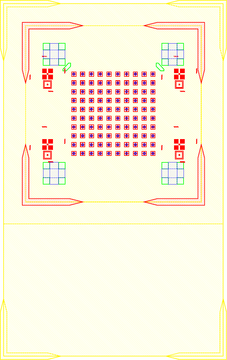
In this section functional LEDs will be used to test the entire process and validate that this process can then later be used to bond a BP with actual transistors. The most major difference between this experiment and the previous ones will be the fact that the LEDs will consist of a ‘mesa’ structure. This structure will require that the electroplating process can complete conformal coating onto the structure.
The GDS files for the LED, BP and overlay of both are in figure


Bonding Issues
Upon attempting to diebond the LED to the backplane, all 3 attempts failed, the remaining BP and LED were withheld to do SEM imaging. From the images taken, it appeared to be that the bonds had a very insufficient thickness of indium present. However, the coating of indium did appear to be conformal.
As seen from the SEM images of the non-bonded samples in figures and the thickness of indium that was generated during the electroplating process was not nearly thick enough for the expected results of $4-6\mu m$. I believe that this was likely an issue that arose due to the poor formation of electric fields during the electroplating process as most other variables were fairly well accounted for.


To analyze this further, 2D electrical simulations were conducted to understand how the electric fields are generated during the electroplating process. The reference code can be seen in the Appendix.
The resulting electric field from the code looks like figure.

Conformation to Theory
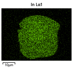
As the theory from the previous section would suggest that there would be a greater flux of indium into the sections near the alligator clip. This can be clearly seen in figure where there is a significant bias of indium near the region with the alligator clip attached.
Development of a Repeatable Process
The existing process failed after verification of previous metrics. As many of the previous issues were resolved methodically, there is likely an inherent flaw with the existing electroplating setup.
To improve the electroplating process I would like to complete the following goals:
Minimize movement of overall system.
Make electric field lines more uniform.
Minimize variability between electroplating runs.
To achieve the previous goals, I would like to propose the following solutions:
Fix the anode(indium bar) into a rigid fixture that maximizes flatness of the bar.
Fix the distance between the anode and cathode with a rigid structure.
Maximize uniformity of the electric fields by ensuring no other conductors are available on the same plane or between the anode and cathode.
To complete these goals a number of 3D models were designed and revised until they could meet the design requirements.
Furthermore, once the designs have been prototyped, it is necessary that appropriate materials are selected to function appropriately in the chemical conditions that the sample experiences.


Since the 3D designs in would meet the specifications indicated earlier, appropriate material selection would be required.
As such materials were selected to meet chemical resistance properties for the harshest chemicals that would be used in the process ($15\% \text{HCl}$). While a variety of plastics met the requirements including PEEK, PTFE, HDPE and many others [@margolis2006engineering], HDPE was selected as it was many orders of magnitude cheaper than PEEK or PTFE and was also much more easily machinable.
This selection would allow for more easy prototyping while meeting all the functional requirements.
Appendix
Appendix A - Standard Operating Procedure Electroplating E3
Purpose
Depositing Indium from an electroplating solution onto samples for die-bonding. The solution used is from Indium Corporation of America and uses their Indium Sulfamate Plating Kit to perform the Indium electroplating.
Equipment
| Name | Quantity |
|---|---|
| Fume Hood | 1 |
| N2 Gun | 1 |
| DI Water Bottle | 1 |
| 2L Beakers | 2 |
| 400mL Beaker | 1 |
| 200mL Beaker | 1 |
| 1L HDPE Bottle | 1 |
| 500mL HDPE Bottle | 1 |
| Hotplate with Magnetic Stirring | 1 |
| Magnetic Stir Bar | 1 |
| Funnel | 1 |
| Insulated Copper Wire | 2 |
| Banana Plug Wires | 2 |
| Copper Alligator Clips | 2 |
| Tweezers kit | 1 |
| Custom Sample Holder | 1 |
| Name | Quantity |
|---|---|
| Indium Sulfamate Plating Bath | 1L |
| Indium Anode (30 cm x 2.5 cm x 1.5 mm) | 1 |
| Sulfamic Acid | 150mL |
| 15-20% HCl | 150mL |
| DI Water | 10L |
| pH Paper Set or pH Meter | 1 |
| Clean Room Wipes Pack | 1 |
Chemical Hazards
No new chemicals are being introduced into the lab, and the SDS of the chemicals relevant to the experiment are attached with the following SOP.
Sulfamic Acid
Indium Sulfamate Plating Bath
Safety Procedure
Lab apron, rubber gloves, safety goggles, face-shield, and closed-toed shoes must be worn before interacting with any chemicals
To avoid spills ready all beakers and bottles under the fume-hood over clean room wipes before opening
Use care when opening and pouring chemicals to avoid spills during the preparation and process of the experiment
Do not touch your face or exposed skin during the process of the experiment
Always wash hands after handling any chemicals or materials
Avoid inhaling the mist or vapour of the chemicals, and avoid exposure to eyes and skin
Perform the entire experiment under a fume hood
Process Flow
Prepare the fume hood surface:
Place clean room wipes on the surface of the fume hood.
Ensure your name and contact information are visible at the work location in case people need to contact you.
Chemicals in the beakers should be identified, and all beakers should be labelled with what chemicals will be in them.
Place the digital hotplate with stirring functionality inside the fume hood.
Do not place a wipe on the hotplate surface. This interferes with the transmission of heat to the beaker and its contents. It may also present a fire hazard. This is regardless of weather the heating element will be used.
Do NOT turn on the heating element over the course of this experiment.
Set all four beakers (2x 2L, 1x 400mL, 1x 200mL) under the fume hood, and set one 2L beaker on the hotplate. Place the stir bar inside the beaker on the hotplate.
Build the Custom Sample Holder and place in the beaker on the hotplate at the appropriate distance for the electroplating process ( 5 cm).
Place the indium anode into the beaker on the hotplate, ensure that there is an appropriate distance from the sample and ensure that the electrode is connected to an alligator clip. Be sure to use fresh gloves when handling the indium electrode to avoid contamination.
Anode/cathode distance may alter grain size and uniformity of electroplating.
It is essential that the sample is perpendicular to the normal of the anode (indium)
Ensure that all PPE is worn appropriately, and no skin is exposed.
Acquire the indium sulfamate solution, sulfamic acid, and diluted HCl solutions from the Acids cabinet and transport it to the fume hood.
Pour the indium sulfamate solution into the beaker on the hotplate.
Ensure that the hotplate is OFF and the beaker is at room temperature to avoid shattering glass
Pour the sulfamic acid into the 200mL beaker
Pour the HCl dilution into the 400mL beaker
Pour 2L of DI water into the remaining large beaker
Turn on stirring to 300RPM
Check the pH of the indium sulfamate solution and verify it is between 1.5 and 2. If the pH exceeds 2 titrate sulfamic acid and mix until the pH enters the range again.
Titration of sulfamic acid into the indium sulfamate solution can be done using a pipette that is labelled and only to be used for sulfamic acid. Since the exact pH is not important titration with a pipette is sufficient and a buret is not required.
Note that all tools used in the titration process must be rinsed with DI water and dried with N2.
Power should ideally be supplied with a pulsed constant current source and set to values in accordance with current over the plating surface area.
Ensure that the power supply is set and ready but disconnected from the sample now.
Measure the surface area of the sample and validate that current supplied to the sample is nominal to $10-20A/ft^2$ or $0.01-0.02A/cm^2$. For the current design this corresponds to nominal values of (0.02A, 0.1V)
Power should be connected as NEGATIVE terminal to sample and POSITIVE terminal to indium anode
Electroplating time is a function of the current density and expected final thickness of the deposited indium.
Rinse the sample with DI water, place into HCl solution for the activation time ( 5 min), rinse again with DI water, and place into the sulfamic acid solution for cleansing ( 3 min).
The sample should be attached to the custom holder
The HCl solution is required for cleaning and acid-activation (see the guide to indium plating).
The sulfamic acid ensures the pH of the base mentalization surface remains acidic and no reformation of oxide occurs.
Place the sample into the plating bath at the appropriate distance and turn on the power supply for the target plating time.
- See the Indium electroplating guide for more information on how this affects the grain size
– Waste disposal, storage instructions for equipment and materials, emergency procedures, and MSDS can be found in the original electroplating SOP document. They were not attached for brevity
Appendix B - Thermal Simulation Code
1
2
3
4
5
6
7
8
9
10
11
12
13
14
15
16
17
18
19
20
21
22
23
24
25
26
27
28
29
30
31
32
33
34
35
36
37
38
39
40
41
42
43
44
45
46
47
48
49
50
51
52
53
54
55
56
57
58
59
60
61
62
63
64
65
66
67
68
69
70
71
72
73
74
75
76
77
78
79
80
81
82
83
%% Define Constants
BP_width   = 6.2 * 10^-3; % m
BP_length  = 6.2 * 10^-3; % m
BP_thickness = 500 * 10^-6; % m

LED_width  = 4.5 * 10^-3; % m
LED_length = 4.5 * 10^-3; % m
LED_thickness = 500 * 10^-6; % m

% http://www.roditi.com/SingleCrystal/Sapphire/Properties.html
SAPPHIRE_THERMAL_CONDUCTIVITY = 25.12; % W / m*K
SAPPHIRE_MASS_DENSITY = 3980; % kg / m^3
SAPPHIRE_SPECIFIC_HEAT = 750; % J / kg * K

AMBIENT_TEMPERATURE = 273.15 + 22; % K
HOTPLATE_TEMPERATURE = 273.15 + 250; % K
CONVECTION_COEFFICIENT_AIR = 5; % Unitless nominal 1-5
% https://www.engineeringtoolbox.com/emissivity-coefficients-d_447.html
EMISSIVITY_COEFFICIENT_SAPPHIRE = 0.8;

%% Define 2D geometry
pderect([(-BP_width/2) (BP_width/2) (-BP_length/2) (BP_length/2)], 'BP')
pderect([(-LED_width/2) (LED_width/2) (-LED_length/2) (LED_length/2)], 'LED')
% Export the geometry description matrix, set formula, and name-space matrix into the MATLAB workspace by selecting
%%%%%%%% Draw > Export Geometry Description, Set Formula, Labels.
% This data lets you reconstruct the geometry in the workspace.


%% Start 3D geometry
g = decsg(gd,sf,ns);
pdegplot(g,"FaceLabels","on")
model = createpde("thermal","transient");
g = geometryFromEdges(model, g)
% Extrude BP
g = extrude(g, BP_thickness);
% Plot
f = figure('Name', 'Geometry');
pdegplot(g,"FaceLabels","on")
view([45 45])

%% Extrude LED
g = extrude(g, 4, LED_thickness);
close(f)
f = figure('Name', 'Geometry');
pdegplot(g,"FaceLabels","on")
view([45 45])

%% Assign geometry to thermal model
model.Geometry = g;
close(f)
f = figure('Name', 'Geometry');
pdegplot(g)


%% Setup Thermal model
thermalProperties(model, ...
    "ThermalConductivity", SAPPHIRE_THERMAL_CONDUCTIVITY, ...
    "MassDensity", SAPPHIRE_MASS_DENSITY, ...
    "SpecificHeat", SAPPHIRE_SPECIFIC_HEAT)
model.StefanBoltzmannConstant = 5.670367e-8;

% Apply heat to the bottom 2 faces
thermalBC(model,"Face", [1 2] ,"Temperature", HOTPLATE_TEMPERATURE);
thermalBC(model,"Face", 3:g.NumFaces, ...
                "ConvectionCoefficient", CONVECTION_COEFFICIENT_AIR, ...
                "AmbientTemperature", AMBIENT_TEMPERATURE, ...
                "Emissivity",EMISSIVITY_COEFFICIENT_SAPPHIRE);

thermalIC(model,AMBIENT_TEMPERATURE);

generateMesh(model);

%% Perform computation for transient thermal analysis
results = solve(model,0:.01:0.3);
%% Plot
for i = 1:length(results.SolutionTimes)
    f = figure(i+5);
    pdeplot3D(model,"ColorMapData",results.Temperature(:,i))
    % clim([AMBIENT_TEMPERATURE HOTPLATE_TEMPERATURE])
    title({['Time = ' num2str(results.SolutionTimes(i)) 's']})
    saveas(f, [num2str(i, '%03.f') '.png']);
end
Appendix C - Electric Field Simulations
Dirty Electric Fields
1
2
3
4
5
6
7
8
9
10
11
12
13
14
15
16
17
18
19
20
21
22
23
24
25
26
27
28
29
30
31
32
33
34
35
36
37
38
39
40
41
42
43
44
45
46
47
48
49
50
51
52
53
54
55
56
57
58
59
60
61
62
63
64
65
66
67
68
69
70
71
72
73
74
%% Define geometry constants
at = 1.1; % aligator clip thickness mm
al = 5; % Length of the aligator clip that sticks out mm
als3 = al*sqrt(3); % assuming aligator clip is at 30deg mm
st = 0.5; % Sample thickness mm
cld = 2; % How much the aligator clip is attached to the sample mm
s_len = 10; % Length of sample mm

scaling = 1/1000;

%% Define geometries
aligator_back_x = scaling*[0 0 0 at at at]; % mm
aligator_back_y = scaling*[0 (als3) (als3+cld) (als3+cld) als3 0]; % mm

aligator_front_x = scaling*[(at+st+al) (at+st+al+at) (at+st+at) (at+st+at) (at+st) (at+st)]; % mm
aligator_front_y = scaling*[0 0 als3 (als3+cld) (als3+cld) als3]; % mm

sample_x = scaling*[at (at+st) (at+st) at]; % mm
sample_y = scaling*[als3 als3 (als3+s_len) (als3+s_len)]; % mm

in_electrode_x = scaling*[(at+50) (at+52) (at+52) (at+50)];
in_electrode_y = scaling*[-5 -5 (50-5) (50-5)];
%% Draw in PDE solver
pdepoly(aligator_back_x, aligator_back_y, 'Aligator_Back');
pdepoly(aligator_front_x, aligator_front_y, 'Aligator_front');
pdepoly(sample_x, sample_y, 'Sample');
pdepoly(in_electrode_x, in_electrode_y, 'Electrode');
pderect([-0.06 0.08 -0.04 0.08], "Conductive_Liquid");

%% Generate PDE Plot
% Export the geometry description matrix, set formula, and name-space matrix into the MATLAB workspace by selecting
%%%%%%%% Draw > Export Geometry Description, Set Formula, Labels.
% This data lets you reconstruct the geometry in the workspace.

g = decsg(gd,sf,ns);

%% Create E Model
emagmodel = createpde("electromagnetic", "conduction");

geometryFromEdges(emagmodel, g)
%% Rest

pdegplot(emagmodel,"EdgeLabels","on", "FaceLabels", "on")

emagmodel.VacuumPermittivity = 8.8541878128E-12;
electromagneticProperties(emagmodel, ...
        "RelativePermittivity",1.00059, ...
        "Conductivity", 1);
%%
electromagneticBC(emagmodel,"Voltage",1.1,"Edge",[6 7 19 20]);
electromagneticBC(emagmodel,"Voltage",0.5,"Edge",[8 9 23 24]);
electromagneticBC(emagmodel,"Voltage",0,"Edge",[1 2 3 4 5 10 11 12 13 14 15 16 17 18 21 22]);


generateMesh(emagmodel);

R = solve(emagmodel);

pdeplot(emagmodel,"XYData",R.ElectricPotential, ...
        "Contour","on", ...
        "FlowData",[R.CurrentDensity.Jx,R.CurrentDensity.Jy])

ali_back_poly = polyshape(aligator_back_x, aligator_back_y);
ali_front_poly = polyshape(aligator_front_x, aligator_front_y);
sample_poly = polyshape(sample_x, sample_y);
in_poly = polyshape(in_electrode_x, in_electrode_y);

hold on;
plot(ali_back_poly);
plot(ali_front_poly);
plot(sample_poly);
plot(in_poly);
axis equal
hold off;
Clean Electric Fields
1
2
3
4
5
6
7
8
9
10
11
12
13
14
15
16
17
18
19
20
21
22
23
24
25
26
27
28
29
30
31
32
33
34
35
36
37
38
39
40
41
42
43
44
45
46
47
48
49
50
51
52
53
54
55
56
57
58
59
60
61
62
%% Define geometry constants
at = 1.1; % aligator clip thickness mm
al = 5; % Length of the aligator clip that sticks out mm
als3 = al*sqrt(3); % assuming aligator clip is at 30deg mm
st = 0.5; % Sample thickness mm
cld = 2; % How much the aligator clip is attached to the sample mm
s_len = 10; % Length of sample mm

scaling = 1/1000;

%% Define geometries
sample_x = scaling*[at (at+st) (at+st) at]; % mm
sample_y = scaling*[als3 als3 (als3+s_len) (als3+s_len)]; % mm

in_electrode_x = scaling*[(at+50) (at+52) (at+52) (at+50)];
in_electrode_y = scaling*[-5 -5 (50-5) (50-5)];

pdepoly(sample_x, sample_y, 'Sample');
pdepoly(in_electrode_x, in_electrode_y, 'Electrode');
pderect([-0.06 0.08 -0.04 0.08], "Conductive_Liquid");

%% Generate PDE Plot
% Export the geometry description matrix, set formula, and name-space matrix into the MATLAB workspace by selecting
%%%%%%%% Draw > Export Geometry Description, Set Formula, Labels.
% This data lets you reconstruct the geometry in the workspace.

g = decsg(gd,sf,ns);

%% Create E Model
emagmodel = createpde("electromagnetic", "conduction");

geometryFromEdges(emagmodel, g)
%% Rest

pdegplot(emagmodel,"EdgeLabels","on", "FaceLabels", "on")

emagmodel.VacuumPermittivity = 8.8541878128E-12;
electromagneticProperties(emagmodel, ...
        "RelativePermittivity",1.00059, ...
        "Conductivity", 1);
%%
electromagneticBC(emagmodel,"Voltage",1.1,"Edge",[3 4 10 11]);
electromagneticBC(emagmodel,"Voltage",0.5,"Edge",[5 6 9 12]);
electromagneticBC(emagmodel,"Voltage",0,"Edge",[1 2 7 8]);


generateMesh(emagmodel);

R = solve(emagmodel);

pdeplot(emagmodel,"XYData",R.ElectricPotential, ...
        "Contour","on", ...
        "FlowData",[R.CurrentDensity.Jx,R.CurrentDensity.Jy])

sample_poly = polyshape(sample_x, sample_y);
in_poly = polyshape(in_electrode_x, in_electrode_y);

hold on;
plot(sample_poly);
plot(in_poly);
axis equal
hold off;
References
1
2
3
4
5
6
7
8
9
10
11
12
13
14
15
16
17
18
19
20
21
22
23
24
25
26
27
28
29
30
31
32
33
34
35
36
37
38
39
40
41
42
43
44
45
46
47
48
49
50
51
52
53
54
55
56
57
58
59
60
61
62
63
64
65
66
67
68
69
70
71
72
73
74
75
76
77
78
79
80
81
82
83
84
85
86
87
88
89
90
91
92
93
94
95
96
97
98
99
100
101
102
103
104
105
106
107
108
109
110
111
112
113
114
115
116
117
118
119
120
121
122
123
124
125
126
127
128
129
130
131
132
133
134
135
136
137
138
139
140
141
142
143
144
145
146
147
148
149
150
151
152
153
154
155
156
157
158
159
160
161
162
163
164
165
166
167
168
169
170
171
172
173
174
175
176
177
178
179
180
181
182
183
184
185
186
187
188
189
190
191
192
193
194
195
196
197
198
199
200
201
202
203
204
205
206
207
208
209
210
211
212
213
214
215
216
217
% uLEDs overview article used in introduction
@Article{uLED_review,
AUTHOR = {Ding, Kai and Avrutin, Vitaliy and Izyumskaya, Natalia and Özgür, Ümit and Morkoç, Hadis},
TITLE = {Micro-LEDs, a Manufacturability Perspective},
JOURNAL = {Applied Sciences},
VOLUME = {9},
YEAR = {2019},
NUMBER = {6},
ARTICLE-NUMBER = {1206},
URL = {https://www.mdpi.com/2076-3417/9/6/1206},
ISSN = {2076-3417},
ABSTRACT = {Compared with conventional display technologies, liquid crystal display (LCD), and organic light emitting diode (OLED), micro-LED displays possess potential advantages such as high contrast, fast response, and relatively wide colour gamut, low power consumption, and long lifetime. Therefore, micro-LED displays are deemed as a promising technology that could replace LCD and OLED at least in some applications. While the prospects are bright, there are still some technological challenges that have not yet been fully resolved in order to realize the high volume commercialization, which include efficient and reliable assembly of individual LED dies into addressable arrays, full colour schemes, defect and yield management, repair technology and cost control. In this article, we review the recent technological developments of micro LEDs from various aspects.},
DOI = {10.3390/app9061206}
}
@article{LCD_bad,
author = {Harbers, Gerard and Timmers, Wim and Sillevis-Smitt, Willem},
title = {LED backlighting for LCD HDTV},
journal = {Journal of the Society for Information Display},
volume = {10},
number = {4},
pages = {347-350},
keywords = {Light-emitting diodes, backlighting, LCD HDTV},
doi = {https://doi.org/10.1889/1.1827889},
url = {https://sid.onlinelibrary.wiley.com/doi/abs/10.1889/1.1827889},
eprint = {https://sid.onlinelibrary.wiley.com/doi/pdf/10.1889/1.1827889},
abstract = {Abstract— Light-emitting diodes (LEDs) are used today for backlighting of small displays such as PDAs and mobile phones. We show in this paper that a new LED technology can be used for high-demanding display-backlighting applications such as LCD HDTV. Using this new type of emitter, called a Luxeon™ Power Light Source, a brightness higher than an edge-lit CCFL backlight can be achieved, while compared to a direct-lit CCFL backlight the thickness is lower and the uniformity is better. With on-going improvements in LED performance over the coming years, LED backlights will reach and even outperform the brightness performance of direct-lit backlights while maintaining the benefits of edge-lit solutions at even higher brightness levels.},
year = {2002}
}
@article{uledhurdles,
author = {Lee, Tzu-Yi and Chen, Li-Yin and Lo, Yu-Yun and Swayamprabha, Sujith Sudheendran and Kumar, Amit and Huang, Yu-Ming and Chen, Shih-Chen and Zan, Hsiao-Wen and Chen, Fang-Chung and Horng, Ray-Hua and Kuo, Hao-Chung},
title = {Technology and Applications of Micro-LEDs: Their Characteristics, Fabrication, Advancement, and Challenges},
journal = {ACS Photonics},
volume = {9},
number = {9},
pages = {2905-2930},
year = {2022},
doi = {10.1021/acsphotonics.2c00285},
URL = {https://doi.org/10.1021/acsphotonics.2c00285},
eprint = {https://doi.org/10.1021/acsphotonics.2c00285}
}
@article{indium_diebonding,
author = {Harbers, Gerard and Timmers, Wim and Sillevis-Smitt, Willem},
title = {LED backlighting for LCD HDTV},
journal = {Journal of the Society for Information Display},
volume = {10},
number = {4},
pages = {347-350},
keywords = {Light-emitting diodes, backlighting, LCD HDTV},
doi = {https://doi.org/10.1889/1.1827889},
url = {https://sid.onlinelibrary.wiley.com/doi/abs/10.1889/1.1827889},
eprint = {https://sid.onlinelibrary.wiley.com/doi/pdf/10.1889/1.1827889},
abstract = {Abstract— Light-emitting diodes (LEDs) are used today for backlighting of small displays such as PDAs and mobile phones. We show in this paper that a new LED technology can be used for high-demanding display-backlighting applications such as LCD HDTV. Using this new type of emitter, called a Luxeon™ Power Light Source, a brightness higher than an edge-lit CCFL backlight can be achieved, while compared to a direct-lit CCFL backlight the thickness is lower and the uniformity is better. With on-going improvements in LED performance over the coming years, LED backlights will reach and even outperform the brightness performance of direct-lit backlights while maintaining the benefits of edge-lit solutions at even higher brightness levels.},
year = {2002}
}
@article{parbrook2021micro,
title ={Micro-Light Emitting Diode: From Chips to Applications},
author ={Parbrook, Peter J and Corbett, Brian and Han, Jung and Seong, Tae-Yeon and Amano, Hiroshi},
journal ={Laser \& Photonics Reviews},
volume ={15},
number ={5},
pages ={2000133},
year ={2021},
publisher ={Wiley Online Library}
}
@techreport{indiumCorpGrainStructure,
author = {},
institution = {Indium Corporation},
title = {Achieving a Finer Grain Structure Using the Indium Sulfamate Plating Bath},
url = {https://www.indium.com/technical-documents/application-notes/download/23/},
year = {2016}
}
@techreport{indiumCorpPulsing,
author = {},
institution = {Indium Corporation},
title = {Indium Bump Electroplating of Wafers Using Pulse Plating },
url = {https://www.indium.com/technical-documents/application-notes/download/2010/},
year = {2016}
}
@techreport{indiumCorpConstants,
author = {},
institution = {Indium Corporation},
title = {Physical Constants of Pure Indium },
url = {https://www.indium.com/technical-documents/application-notes/download/358/},
year = {2022}
}
@techreport{indiumCorpPlating,
author = {},
institution = {Indium Corporation},
title = {Plating, an Alternative Method of Applying Indium },
url = {https://www.indium.com/technical-documents/application-notes/download/1994/},
year = {2018}
}
@techreport{indiumCorpSurfacePrep,
author = {},
institution = {Indium Corporation},
title = {Proper Surface Preparation For Indium Plating },
url = {https://www.indium.com/technical-documents/application-notes/download/29/},
year = {2016}
}
@techreport{indiumCorpBath,
author = {},
institution = {Indium Corporation},
title = {Prototype Plating Using Indium Sulfamate Plating Bath },
url = {https://www.indium.com/technical-documents/application-notes/download/299/},
year = {2016}
}
@inbook{waferBondingHandbook,
author = {Koyanagi, Mitsumasa and Motoyoshi, Makoto},
publisher = {John Wiley \& Sons, Ltd},
isbn = {9783527644223},
title = {Eutectic Au-In Bonding},
booktitle = {Handbook of Wafer Bonding},
chapter = {8},
pages = {139-159},
doi = {https://doi.org/10.1002/9783527644223.ch8},
url = {https://onlinelibrary.wiley.com/doi/abs/10.1002/9783527644223.ch8},
eprint = {https://onlinelibrary.wiley.com/doi/pdf/10.1002/9783527644223.ch8},
year = {2012},
keywords = {three-dimensional integration, large-scale integration, eutectic AuIn bonding, epoxy adhesive injection, high-density AuIn microbumps},
abstract = {Summary This chapter contains sections titled: Introduction Organic/Metal Hybrid Bonding Organic/In-Au Hybrid Bonding Three-Dimensional LSI Test Chips Fabricated by Eutectic In-Au Bonding High-Density and Narrow-Pitch Mirco-bump Technology}
}
@techreport{diebonderDatasheet,
author = {},
institution = {Dr. TRESKY AG},
title = {Die Bonder T-3000-FC3 Datasheet},
url = {https://qnfcf.uwaterloo.ca/equipment/packaging-lab-qnc-1706-1/die-bonder-tresky-diebond/manuals/vendor/2033654-pr-t-3000-fc3.pdf/view},
year = {2008}
}
@techreport{RemoverPGds,
author = {},
institution = {Kayaku Advanced Materials},
title = {Remover PG Technical Data Sheet},
url = {https://kayakuam.com/wp-content/uploads/2020/11/KAM-Remover-PG-TDS.10.29.20-final.pdf},
year = {2020},
month = {11}
}
@article{deppisch2006material,
title={The material optimization and reliability characterization of an indium-solder thermal interface material for CPU packaging},
author={Deppisch, Carl and Fitzgerald, Thomas and Raman, Arun and Hua, Fay and Zhang, Charles and Liu, Pilin and Miller, Mikel},
journal={Jom},
volume={58},
pages={67--74},
year={2006},
publisher={Springer}
}
@techreport{AZPdatasheet,
author = {},
institution = {AZ Electronic Materials},
title = {AZ ® P4620 Photoresist Data Package},
url = {https://www.microchemicals.com/micro/tds_az_p4620_photoresist.pdf},
year = {2014},
}
@techreport{daisychainTest,
author = {},
institution = {TopLine Corporation},
title = {Understanding Benefits of Daisy Chain},
url = {https://www.topline.tv/daisychain.html},
year = {2023}
}
@misc{CrAuPresentation,
author = {Pranav Gavirneni},
institution = {University of Waterloo},
title = {DEV-OI-0010, DEV-PG-0029 Wafer Process Traveller},
year = {2021},
month = {6}
}
@techreport{oxide_breakdown,
author = {},
institution = {EE Semi},
title = {Oxide Breakdown},
url = {https://www.eesemi.com/oxidebreakdown.htm},
year = {2004}
}
@article{plasma_clean_oxide,
title={Two-Step Plasma Process for Cleaning Indium Bonding Bumps},
url={https://ntrs.nasa.gov/citations/20090022331},
journal={NASA Tech Briefs, June 2009},
author={Greer, Harold F. and Vasquez, Richard P. and Jones, Todd J. and Hoenk, Michael E. and Dickie, Matthew R. and Nikzad, Shouleh},
year={2009},
month={6}
}
@book{margolis2006engineering,
title={Engineering plastics handbook},
author={Margolis, James M},
year={2006},
publisher={McGraw-Hill Education}
}
The LED and backplane are in quotes as these are not actual LEDs or backplanes with transistors, but instead are mock samples with similar physical characteristics. Those characteristics being the sample size and the $\text{In}-\text{Au}$ coating on the samples. Differences arise from the lack of a MESA structure that will be seen in the successive chapter [sec:BondingToLEDS]{reference-type=”ref” reference=”sec:BondingToLEDS”} ↩
Gimbal diebonding head is used to minimize non-uniformity of bonding pressure over the surface of the sample ↩
Due to the limitations of the diebonder in the packaging lab, alignment must be done on only one section of the viewfinder. This is due to the non-planar alignment of the optical path in the flip-chip camera. ↩
The material and strength properties of the bond will be discussed further in the chapter in section 14{reference-type=”ref” reference=”sec:Ch2_repeatable”} ↩